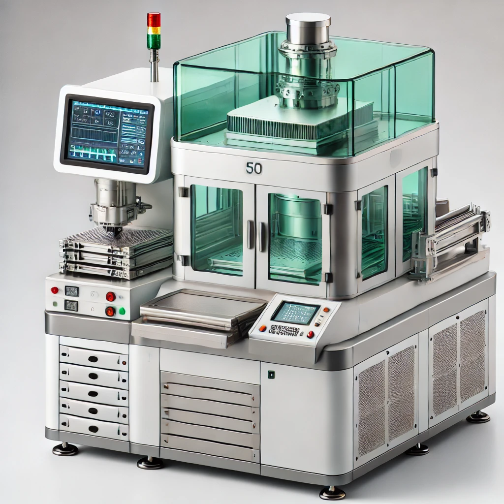
Fluxless TCB vs TCB
As interconnection pitches shrink below 10µm for advanced logic and memory applications, fluxless TCB solves the issues that standard TCB encounters with the flux.
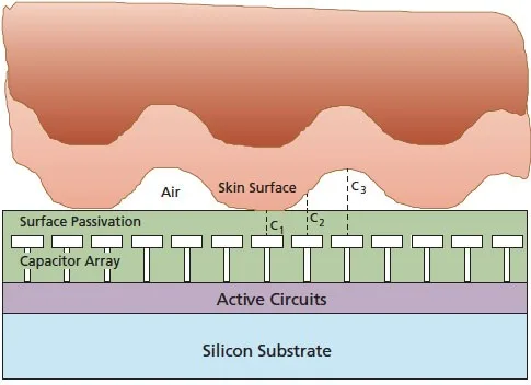
Surface passivation in semiconductors refers to a process of protecting the surfaces of semiconductor materials from external contaminants and unwanted interactions by applying a layer or coating. Just like we use sunscreen to protect our skin from the harmful effects of the sun, surface passivation provides a protective layer to shield the semiconductor material from external harms.
Semiconductors have very sensitive surfaces that can easily be damaged or affected by factors such as moisture, impurities, or even tiny particles. This can cause the performance of the semiconductors to degrade or even fail altogether. To prevent this, a coating, normally silicon nitride (Si3N4) or silicon dioxide (SiO2), is applied to the surface of the semiconductor. This layer acts as a barrier, preventing any harmful substances or unwanted electrical interactions from reaching the semiconductor material. It helps to keep the semiconductor clean, stable, and reliable. The surface passivation process ensures that the semiconductor can function properly, allowing it to perform its intended functions effectively and reliably.
The surface passivation method was pioneered by Mohamed M. Atalla, an engineer from Bell Labs, in 1959. Mr. Atalla is also known for achieving important discoveries in MOSFET, a type of semiconductor transistor. For a comprehensive overview about the history of surface passivation and Mr. Atalla check this Wikipedia link.
Let´s imagine a semiconductor manufacturer, Passive Semiconductor Inc, that is experiencing problems with low yield and high leakage current in their power devices. The company starts examining their manufacturing process and identifies surface passivation as a possible issue. They find that their current passivation method is not providing sufficient protection from environmental and mechanical damage, leading to device failure and corrosion.
To address this issue, Passive Semiconductor Inc developes a new process that utilizes a high density plasma (HDP) deposition method. This process involves depositing a thin layer of silicon oxynitride (SiON) on the surface of the device to provide a protective layer while maintaining electrical stability.
The new process is implemented and the performance of the power devices is measured. The results show a significant improvement in yield and a decrease in leakage current and corrosion. The devices also exhibit improved reliability and stability over a range of operating conditions. These results are achieved because the new SiON passivation layer provides better protection against chemical species such as moisture and hydrocarbons, which can degrade the surface of the device, thereby reducing device performance.
The company continues to refine its surface passivation process, optimizing the thickness and quality of the SiON layer to further improve performance. This results in even higher quality of devices with lower leakage current and higher long term.

As interconnection pitches shrink below 10µm for advanced logic and memory applications, fluxless TCB solves the issues that standard TCB encounters with the flux.
The metal pitch refers to the distance between the centers of two adjacent metal interconnect lines on an integrated circuit (IC). Since transistors evolved into 3D strucrures, this measurement has lost significance.
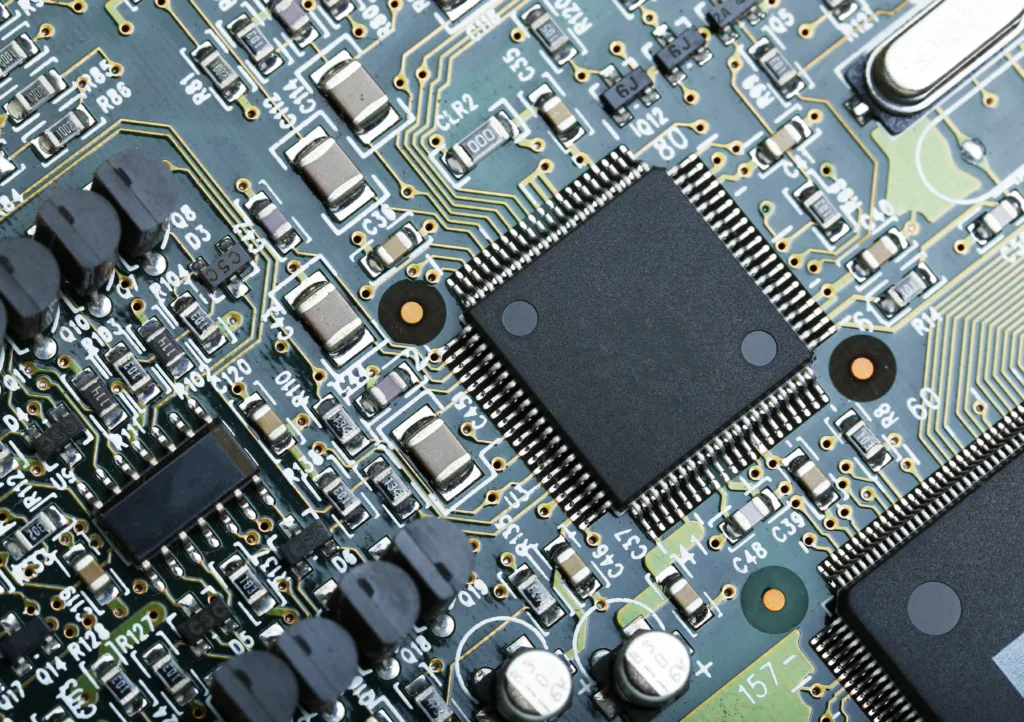
The front-end and back-end are highly interdependent. A constant feedback loop between front and back-end engineers is necessary to improve manufacturing yields.

Built directly into the silicon, through silicon vias (TSV) facilitate 3D IC integration and allow for more compact packaging. They have become the default solution to interconnect different chip layers or to stack chips vertically.
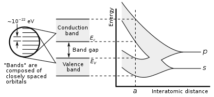
Silicon carbide (SiC) is used in electric vehicles due to its wide bandgap and great thermal conductivity. Gallium nitride (GaN) shares many characteristics with SiC while also minimizing RF noise.
GPU vs CPU is a parallelization vs complexity dilemma. While GPUs can manage very large parallel calculations, they struggle with linear, more heterogeneous tasks, where CPUs excel.